FPGA, DSP, and Ultra High Speed ADC experts
High Gain,
High Bandwidth, and Low-Noise Amplifier
Designed and PCB layout a differential amplifier board with Gain = 80dB and BW = 1GHz. The amplifier is part of a Receiver analog front-end and it interfaces to a multi-Gsps Analog-to-Digital Converter. The amplifier maximum output voltage swing can be up to 4.75V.
76-Channels, 1-Gsps, 8-bits ADC unit
System design involves a low jitter PLL clock source with low skew clock distribution techniques to synchronize all 76-channels A/D Converters. All A/D Converters are synchronously running at 1-Gsps and the sample data is pre-processed by Channel-FPGA (Virtex-E) in real-time. The unit also implemented few other FPGAs to perform various control as well as communication among all FPGAs and the Host computer.
 96-Channel,
2-Gsps Threshold detection unit
Receiver for a Terrestrial-Mapping system with a 96-pixels detector which
reports laser pulse returns simultaneously. All 96-pixels are
synchronously running at 2GHz and report a range resolution up to 7.5cm.
Project involves high speed opto-electronics, High-Voltage (up to 5KV) and
high-efficiency Power suppliers, Thermal management, Clock-distribution, and
FPGA designs. All controls and communication functions are performed by
few Xilinx Virtex-2 FPGAs.

6-Gsps, 8-bit Analog-to-Digital
Converter Board
Applying ultra high speed analog (RF) and digital design techniques to sample >GHz analog signal, buffer, process, and store the sampled data through a Virtex-5 FPGA. FPGA applies Digital Signal Processing algorithm to pre-process the data and interface with the Host with PCI-Express or High-Speed USB (480Mbps) interface. Design also implemented DDR2 memories.
Realtime
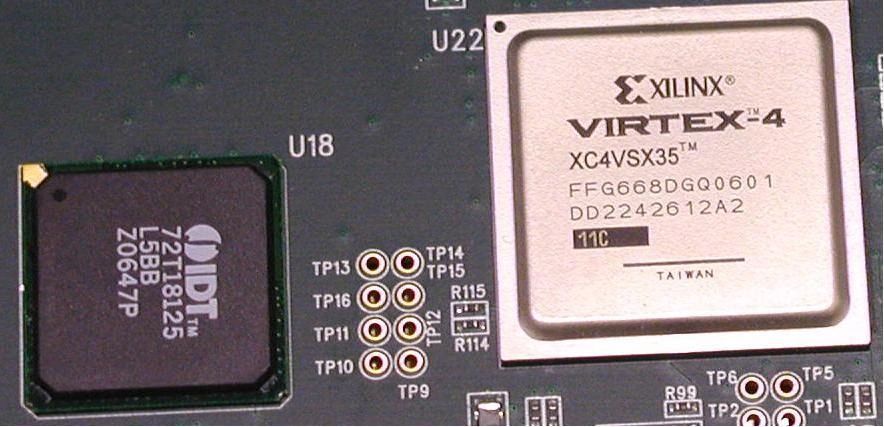
FFT Processing Board with Xilinx Virtex-4 FPGA
The Board continuously sampled and digitized input signal to a 250MHz, 12-bit
data. The on-board Virtex-4 FPGA then, converts the sampled data to
a 128-tags FFT in every 512ns. The FFT data is processed with other DSP
routines in real-time and is output to the Host through a High-Speed USB interface.
TMS320C31 Based Tele-Conference unit
etc.

 76-Ch
76-Ch